The Role of Automated Optical Inspection (AOI) in PCB Fabrication: Ensuring Quality and Efficiency

In the intricate world of electronics manufacturing, printed circuit boards (PCBs) are the foundation of modern devices, acting as the nervous system of gadgets ranging from smartphones to industrial machinery. To ensure that PCBs meet the stringent quality standards required for flawless performance, automated optical inspection (AOI) has emerged as an indispensable technology. AOI plays a crucial role in PCB fabrication and assembly, ensuring that products are free of defects and ready for deployment.
What Is Automated Optical Inspection (AOI)?
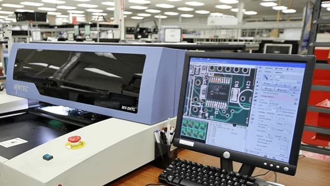
Automated optical inspection (AOI) is a machine-driven process that utilizes advanced imaging systems and algorithms to examine PCBs for defects. It inspects surface defects, dimensional inaccuracies, and component placement issues that would be challenging or impossible to identify through manual inspection, especially given the increasing complexity and miniaturization of modern PCBs.
AOI employs high-resolution cameras and image processing software to detect manufacturing faults, such as:
• Soldering defects (e.g., shorts, insufficient solder).
• Misaligned or missing components.
• Open circuits and broken traces.
By automating this critical inspection process, AOI ensures consistent quality control, reducing costs and improving efficiency in the production line.
How AOI Works in PCB Manufacturing
1. Inspection After PCB Fabrication
Once a bare PCB is fabricated, AOI checks for manufacturing defects like:
• Surface defects: Nodules, scratches, or contamination.
• Dimension defects: Open circuits, short circuits, or irregular line widths.
2. Inspection During PCB Assembly
In assembly, AOI inspects the placement and soldering of surface-mount components (SMT) and through-hole components. It identifies defects such as:
• Incorrectly placed components.
• Insufficient solder joints.
• Tombstoning (where components stand vertically on the PCB).
• Solder bridging (unintentional connections between solder pads).
Advantages of AOI in PCB Fabrication
1. High Positional Accuracy
With the miniaturization of electronic components, the precision of AOI systems is paramount. Modern AOI systems use sub-pixel accuracy to detect minuscule positional deviations, ensuring that even the smallest components are correctly placed and soldered.
2. Cost-Effective Quality Control
Detecting and rectifying defects early in the manufacturing process reduces waste and minimizes rework costs. AOI’s ability to catch errors before mass production ensures that faulty designs are not replicated, saving significant time and money.
3. Multiple Inspection Capabilities
AOI can inspect bare PCBs for manufacturing defects and assembled PCBs for component placement and soldering issues. This versatility makes it a critical tool throughout the PCB production lifecycle.
4. Programmable Lighting
Lighting plays a crucial role in achieving optimal inspection results. AOI systems use programmable, dynamic lighting to enhance defect detection, employing multiple colors and angles to highlight issues. This adaptability ensures comprehensive coverage of various defect conditions.
5. Network-Capable Software
Modern AOI systems collect and store inspection data in various formats, including images, text, and databases. This data can be analyzed to identify recurring issues and optimize manufacturing processes. Network integration allows seamless retrieval and sharing of this information across production lines.
6. Flexibility Across Production Stages
AOI can be implemented at multiple stages of PCB production, from fabrication to assembly and even post-soldering. Its adaptability allows manufacturers to target specific areas of concern, enhancing overall efficiency and product quality.
Why AOI Is Critical for Modern PCB Manufacturing
Early Detection of Defects
AOI provides a vital quality gate in PCB production, catching errors before they propagate through the manufacturing process. This early detection reduces waste and ensures that only high-quality boards reach the final stages of production.
Handling Complex Designs
As PCBs become more compact and feature-dense, manual inspection becomes impractical. AOI’s automated precision is indispensable for identifying defects in intricate designs that would be impossible to verify visually.
Ensuring Product Reliability
A faulty PCB can compromise the functionality of an entire electronic device. By ensuring the accuracy and quality of PCBs, AOI directly contributes to the reliability of end products.
How Automated Optical Inspection (AOI) Works in PCB Fabrication
Automated Optical Inspection (AOI) is a critical process in PCB fabrication and assembly, ensuring that circuit boards meet stringent quality standards. It uses advanced imaging and machine-learning techniques to inspect PCBs for defects. Here’s an in-depth look at how AOI works in PCB manufacturing.
Before the AOI system starts inspecting, it must be programmed with the design data and inspection parameters. This involves:
• Loading the PCB Design File: The PCB design files (like Gerber files) or CAD data are imported to guide the inspection process.
• Defining Inspection Parameters: Critical areas of inspection, such as solder joints, component placement, and traces, are defined. Specific defect criteria, including dimensional tolerances and alignment standards, are programmed.
2. Image Capture
The AOI system captures high-resolution images of the PCB for analysis. This involves several key elements:
• High-Speed Cameras: These cameras scan the board and capture detailed images of its surface.
• Programmable Lighting: Multi-angle and multi-color lighting highlight specific features, such as solder joints or component leads. Proper lighting ensures that even subtle defects are visible.
3. Image Processing
After capturing the images, the AI based software system processes them to identify potential defects. This step involves:
• Comparing with Design Data: The captured images are compared to the reference data (ideal PCB design). Any deviations are flagged for review.
• Algorithm-Based Detection: Advanced algorithms analyze features like component placement, solder joint quality, and trace continuity.
• Pattern Matching: The system recognizes patterns and checks them against predefined standards to identify issues like missing components or incorrect polarity.
4. Defect Classification
Detected issues are categorized into defect types, such as:
• Surface Defects: Scratches, contamination, or nodules.
• Dimensional Defects: Open circuits, short circuits, or line width violations.
• Assembly Defects: Missing, misaligned, or damaged components, solder bridging, or lifted leads.
Defects are typically classified as critical (requiring immediate attention) or non-critical (for review or rework).
5. Output and Reporting
The AOI system provides a detailed report of its findings, which includes:
• Images of Detected Defects: Highlighting areas requiring attention.
• Data Logs: Information on defect locations, types, and severity.
• Suggestions for Rework: Based on the type and location of the defect.
This data can be used to improve manufacturing processes and minimize recurring errors.
6. Feedback
In modern manufacturing, AOI systems are often integrated into a feedback loop. When defects are identified, the system generate the following alerts:
• Signal the Production Line: Halt the process to prevent further defects.
• Provide Real-Time Feedback: Adjust manufacturing parameters, such as soldering temperature or placement alignment, to correct the issue.
Applications of AOI in PCB Manufacturing
1. Short Circuits and Line Violations
AOI ensures that traces on the PCB adhere to specified design rules, detecting issues like short circuits and line width violations that could cause malfunctions.
2. Component Placement
By verifying that each component is accurately placed and soldered, AOI reduces the risk of functional failures in the final product.
3. High-Frequency and Power Applications
In specialized PCBs designed for high-frequency or high-power applications, AOI ensures compliance with stringent design standards, preventing performance issues.
Future Trends in AOI
As technology evolves, AOI systems are expected to become even more sophisticated, incorporating advancements such as:
1. AI-Powered Inspection
Artificial intelligence and machine learning algorithms will enable AOI systems to analyze data more intelligently, identifying patterns and predicting potential defects with greater accuracy.
2. 3D AOI Systems
Traditional 2D AOI systems are being complemented by 3D systems that provide volumetric data. This enhancement allows for more precise detection of defects like insufficient solder paste and lifted leads.
3. Integration with IoT
Connected AOI systems will integrate seamlessly with the Internet of Things (IoT), enabling real-time monitoring and remote control of inspection processes.
4. Enhanced Data Analytics
Future AOI systems will offer advanced data analytics tools, providing insights into production trends and facilitating continuous improvement in manufacturing processes.
Automated optical inspection (AOI) is a cornerstone of modern PCB fabrication, combining precision, speed, and adaptability to meet the challenges of today’s complex designs. By ensuring early defect detection, enhancing product reliability, and reducing costs, AOI has become an essential tool for manufacturers striving for excellence in electronic production.
As PCB technology continues to evolve, so too will AOI systems, incorporating innovations like AI and 3D imaging to keep pace with industry demands. For businesses in the PCB industry, investing in robust AOI systems is not just a necessity—it’s a commitment to quality and a competitive edge in an ever-evolving market.


